Custom Electronic Circuit Design Services - Digital & Analog Design - Embedded System Design -
PCB Design and Layout - PCB Manufacturing - PCB Cloning / Reverse Engineering


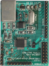
Example of the design of a PCB
- CAD design of the PCB
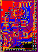
- PCB once manufactured and assembled
Basic guidelines for reducing PCB cost
PCB manufacturing costs depend on several factors that must be taken into account during the design process. If you are a newbie in the PCB field, maybe your design is not optimized from a cost standpoint. The majority of beginner PCB designers don’t consider basic width, spacing and many other rules that have a big impact not only in the tooling costs but also in the unit prices.
If you want to keep your tooling and manufacturing costs to a minimum we recommend you to follow our recommendations that are listed in this article.
1.- Rule of thumb for board size:
Try to keep the board size or area to a minimum.
This is the most obvious rule. Costs tend to go up when the board size is bigger. You can think that price is approximately proportional to the board’s area.
2.- Rule of thumb for board shape and slots:
Unless necessary try to use standard board shapes like squares and rectangles given the fact that irregular shapes may introduce extra cost. Try to avoid slots (internal cutouts) unless necessary for mounting purposes.
Some PCB fab shops charge additional costs for irregular shapes that are different from standard shapes as squares or rectangles. Figure 1 depicts a PCB with an irregular shape that can be used for mounting purposes inside a custom enclosure for a custom system. If the PCB shape is not important we recommend designing boards with square or rectangular shapes for reducing costs.
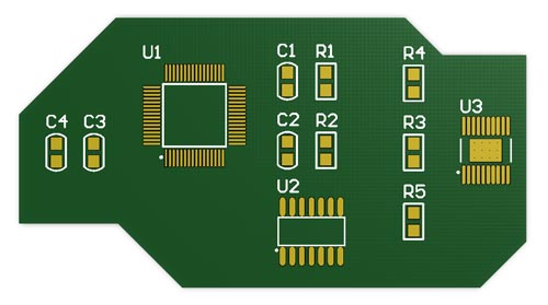
Fig 1. A PCB with an irregular shape
Figure 2 shows a printed circuit board with a rectangular slot. PCB fab shops charge you an extra cost for making cutouts on the board, so if it is not mandatory to have slots we recommend you not to use them.
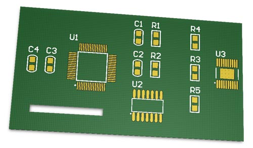
Fig 2. A rectangular PCB with an internal cutout or slot
3.- Rule of thumb for the size of copper objects and the spacing between them:
As the physical dimensions of copper objects and spacing between them decrease, the cost increases.
This one works in the opposite direction to first rule of thumb (now the bigger the cheaper). This rule makes a lot of sense, because for printing smaller objects on copper you need machines with better precision and smaller tolerances. More precision means more cost, and this increase could be important especially for low quantities and prototypes.
When we talk about physical dimensions of copper objects we are referring to pads (SMD and thru-hole), tracks, vias and any object printed on a copper layer. For the case of tracks and pads figure 3 shows this idea. The spacing between pads is denoted as dP and the spacing between tracks as dT while the track's width is denoted as wT. The majority of PCB fab shops consider a board as standard (no extra cost involved) when min(dP), min(dT) and min(wT) are between 8 to 10[mils] (0.2[mm] to 0.254[mm] approx). So for reducing costs it would be a good idea to constrain your design to these values. EDA software generally have a section where you can enter physical rules, which once entered are constantly checked by the DRC (design rule check) system for avoiding out-of-rule errors.
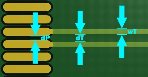
Fig 3. Spacing between pads and between tracks
4.- Rule of thumb for holes:
The smaller the holes and annular rings, the bigger the price.
Try to use always the bigger diameter possible for holes. Manufacturing smaller holes involves the use of more precise machinery which increases costs in an important way. As a reference, some manufacturers charge you an extra cost if you need holes smaller than 0.4[mm]. But in general, for determining which is the minimum hole size for an standard PCB (which does not include extra cost) you must ask your PCB manufacturer. For this article we are going to denote a hole's diameter by dH.
There is an important specification called minimum annular ring that applies only to thru-hole pads and vias, which is defined as the minimum distance between the hole's border and the pad's border, or in other words, the minimum width of the copper ring that confines the hole. You can see this concept in figure 4 and figure 5 for a better understanding. Figure 4 shows the minimum annular ring concept for a round thru-hole pad or via, while figure 5 shows the same idea but for an oblong shaped pad.
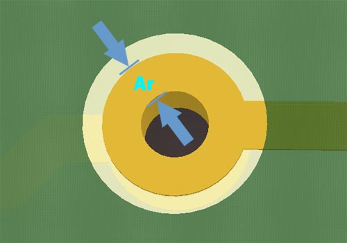
Fig 4. Annular ring concept for a round thru-hole pad or via
It's important to note that in the case of a round thru-hole pad or via the annular ring width is homogeneous around the hole. In the case of the oblong thru-hole the width is not homogeneous around the hole. The minimum annular ring corresponds to the section indicated by the red marker shown in figure 5.

Fig 5. Minimum annular ring concept for an oblong shaped thru-hole pad
If the minimum annular ring is under the standard specs of your PCB manufacturer the cost will be increased and in some cases it could be important, so it is very important to add this rule to your EDA software before designing your PCB. As a reference, some manufacturers charge you an extra cost if you need minimum annular rings smaller than 0.3[mm], but it is always a good idea to contact your manufacturer and ask them which is the minimum value for this variable so it can be considered as a standard value (no extra cost involved).

Fig 6. Minimum annular ring and hole diameter of an oblong pad
With the aid of figure 6 we can establish the following simple equation that relates the pad's size, minimum annular ring and hole size. The equation is as follows:
PadMinSize = 2*min(Ar)+dH
With this equation you can calculate the minimum size that a pad can have given the minimum annular ring and minimum hole diameter. As an example suppose that dH=0.4[mm] and min(Ar)=0.3[mm], hence PadMinSize=1[mm]. So any thru-hole pad smaller than 1[mm] (for this example) will produce extra costs.
It's always a good idea to consider in the equation a little margin because in the real world, machines have tolerances greater than cero. So as a summary we can write the minimum pad size equation as:
PadMinSize = 2*min(Ar)+dH+margin
As a reference the margin could have values between 0.05[mm] to 0.1[mm].
A short note about vias:
As shown in our previous article Printed circuit board basic concepts there are basically 3 types of vias: through-hole vias, blind vias and buried vias. Blind and buried vias are used for high density and high frequency complex boards (more on this in a later article). If your design is not of these types don't use them, they are more expensive than normal through-hole vias.
Don't forget to check the minimum specs for a standard PCB with your manufacturer. All the values given here are to be taken as a reference only.
Hope this article helps you in your next or current design.
Thanks for reading!
Eng. M. Patricio Cohen
Electrosoft Engineering
Please click in the following link for going back to our home page: