Custom Electronic Circuit Design Services - Digital & Analog Design - Embedded System Design -
PCB Design and Layout - PCB Manufacturing - PCB Cloning / Reverse Engineering

Example of the design of a PCB
- CAD design of the PCB
- PCB once manufactured and assembled
Electronic Circuit Designs made by us
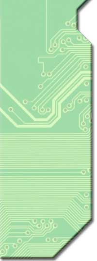
Here you can find some examples of the PCB designs we have made. A printed circuit board can have several layers depending on the complexity of the design.
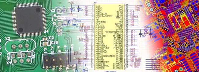
Today we find in the market a huge variety of integrated circuits ( IC's) like microcontrollers, FPGA's and integrated circuits for special applications ( ASICS ) that have built-in several functions and peripherals. All of these integrated peripherals are possible because of the high integration levels (transistors / surface unit) that can be achieved today by IC manufacturers.
Including a great variety of peripherals and functions increases the number of pins found in the integrated circuit packages in an important factor. This is one of the reasons for the printed circuit boards to contain several layers for signal routing. But, the main reasons for PCB's to have many layers are due to negative effects that appear with the high frecuency of operation of today's devices. Designing a PCB to be reliable at high frequencies involves the use of design practices for minimizing the detrimental effects that arise with the increasing frequency. One of these design practices is to incorporate the use of multilayer printed circuit boards for achieving a good signal integrity and also for minimizing the electromagnetic emissions that generate EMI ( electromagnetic interference ) in neighbor electronic systems.
The examples 3 and 4 are high frequency PCB's. That's why we used 6 and 4 layers respectively for these designs.
Examples of Printed Circuit Board Designs |
|
|---|---|
Ex1.a) CAD design of a 2 layer PCB |
Ex1.b) The 2 layer PCB once manufactured |
 |
 |
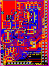
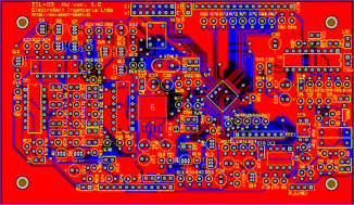
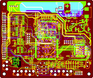
Ex2.a) CAD design of another 2 layer PCB |
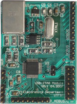
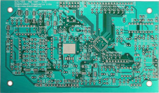
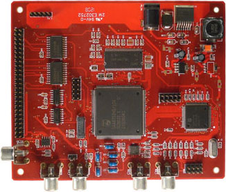
Ex2.b) The 2 layer PCB once manufactured and assembled |
 |
 |
Ex3.a) CAD design of a high speed 6 layer PCB |
Ex3.b) The 6 layer PCB once manufactured and assembled |
 |
 |
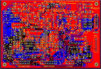
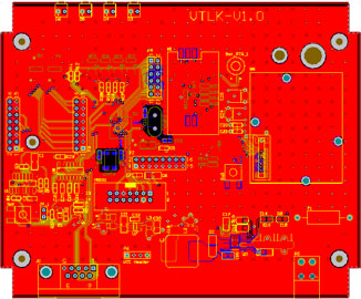
Ex4.a) CAD design of a 4 layer PCB. This PCB is the mainboard of a telemetry system |
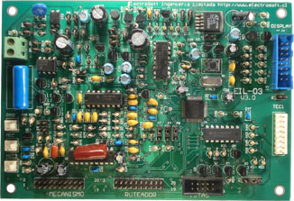
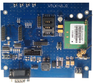
Ex4.b)The 4 layer PCB once manufactured and assembled |
 |
 |
As noted before, when a device operates at high frequencies, several negative effects may arise and make the system not to work at all if they aren't taken in consideration during the layout process. Degradation of digital signals occurs mainly because of transmission line mismatching, crosstalk, ground bounce and rail collapse concepts.
In mixed signal systems (that is, analog and digital) the analog signals can be contaminated with noise from the digital electronics as well from the electromagnetic radiation caused by a nearby wireless device (i.e. Cell phone, bluetooth, etc). Taking these noise sources in consideration makes necessary to use several techniques during the design to minimize interferences, or in technical words, to minimize the electromagnetic susceptibility of the circuit.
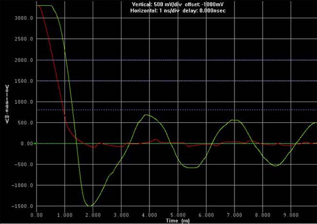
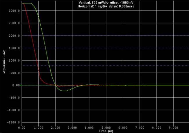
As an example, you can see below some images that show the huge difference that exists between a mismatched transmission line and a matched one. Example 5 shows a simulation of a falling edge produced by a driver without matching and with matching.
A transmission line without matching is going to produce ringing noise in your signal traces because of reflections, as you can see in Ex5.b. If the noise's amplitude is near the logic thresholds, then the receiver may confuse a logic 0 with a logic 1 or vice versa. Or in the case of a clock signal, the device may get double triggered. Of course, these are very bad news for the design engineer if he/she finds these kinds of problems once the board has been manufactured and assembled. Care must be taken from the very beginning.
Examples of transmission line simulations for signal integrity |
|---|
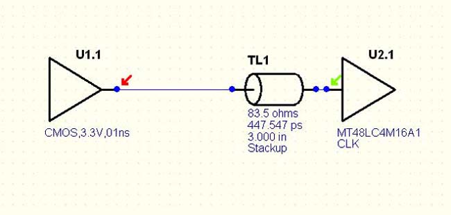
Ex5.a) Schematic of a mismatched transmission line |
 |
Ex5.b) Simulation results of the mismatched transmission line |
 |
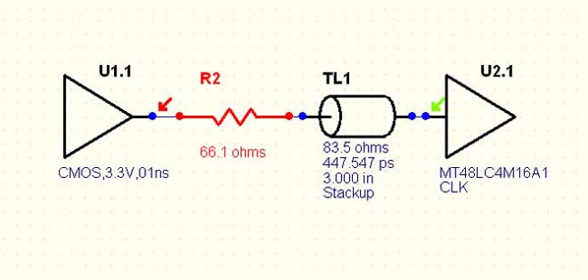
Ex6.a) Schematic of the transmission line with impedance matching |
 |
Ex6.b) Simulation results of the impedance matched transmission line |
 |
We have a section of technical articles that we are currently developing, for visiting it please click in the following link: Electrosoft Engineering Articles about PCB design and layout
Please click in the following link for going back to our home page.